RA1: Fan-Out Wafer-Level Packaging (FOWLP) for future High-Performance Computing (HPC) systems (*Ongoing)
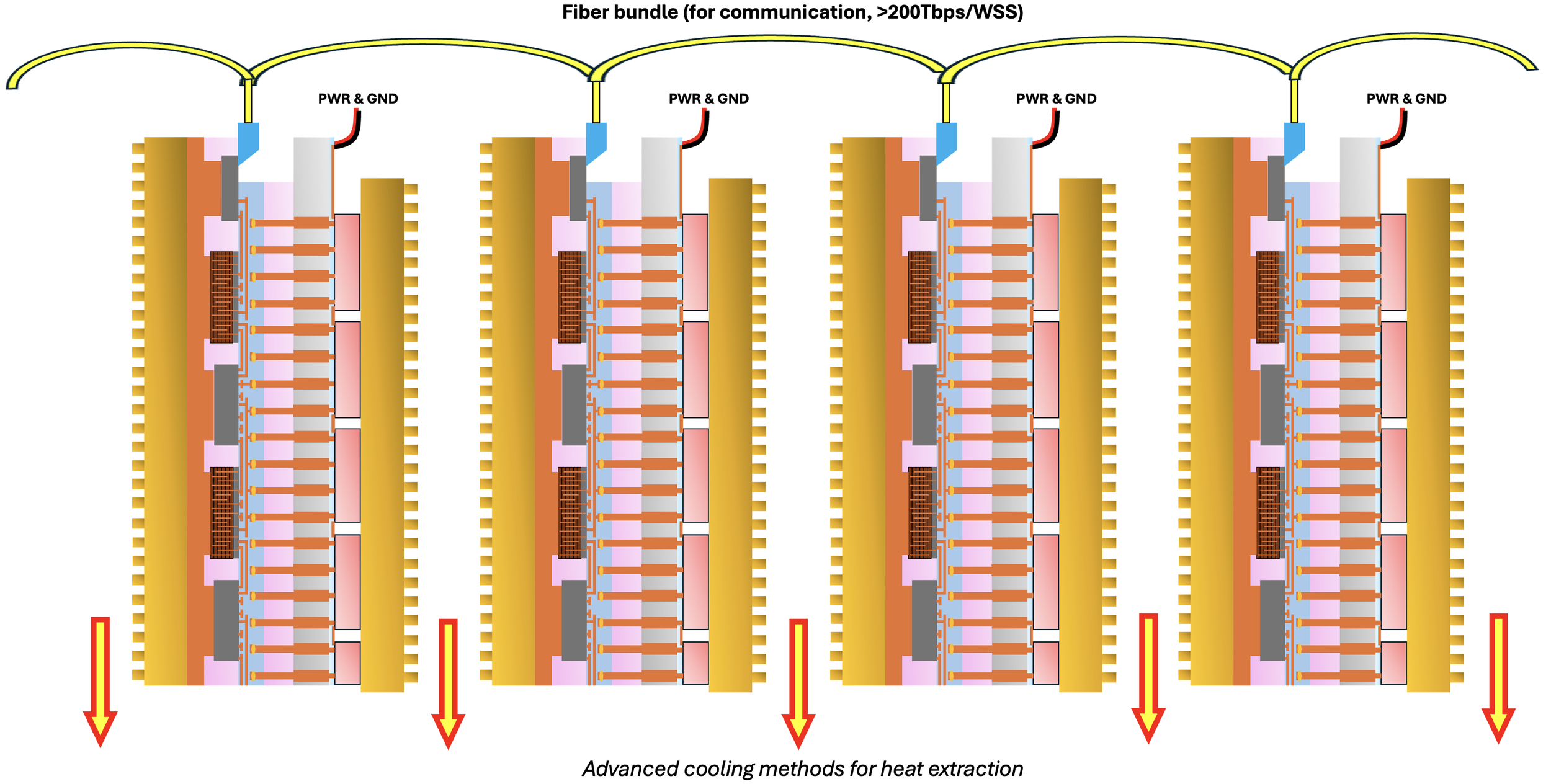
As the semiconductor industry approaches the physical limits of Moore's Law, the focus has shifted from transistor scaling to advanced packaging and heterogeneous integration (HI) as key enablers for future high-performance computing (HPC). While exponential device scaling has driven progress for decades, the slower scaling of package dimensions particularly bump & wiring pitches has become a critical bottleneck, limiting the performance of modern chips due to link latencies & power loss. Conventional packaging, with its coarse interconnects and longer link lengths, relies on energy-hungry SerDes for high-data-rate communication, leading to significant power losses and latency. Fan-Out Wafer-Level Packaging (FOWLP), with fine-pitch, high-density interconnects, and embedded bare-die components without the use of solder offers a potential solution. FOWLP enables seamless integration of heterogeneous components like compute and 3D-stacked memory chiplets with high BW-density interconnection. Conventional FOWLP like TSMC’s InFO has however struggled to push the wiring pitches to less than 10 microns due to issues like die-shift and warpage. At UCLA, we have developed a novel FOWLP process called FlexTrateTM that uses PDMS as the substrate. The unique mechanical properties of viscoelastic PDMS along with novel adaptive lithographic techniques allows us to minimize die-shifts & warpage effects and push the wiring pitches to < 2 microns (‘Scale-down’). The use of a compliant substrate such as PDMS for building the package of the HPC system has additional benefits like minimizing chip-package interactions, improving the thermo-mechanical performance & reliability. This work is still in progress; a conceptual illustration of a HPC system built using this approach is shown in the Figure below.
Research Areas

Compliant-substrate HPC system using FOWLP ( Scale-down & Scale-out)
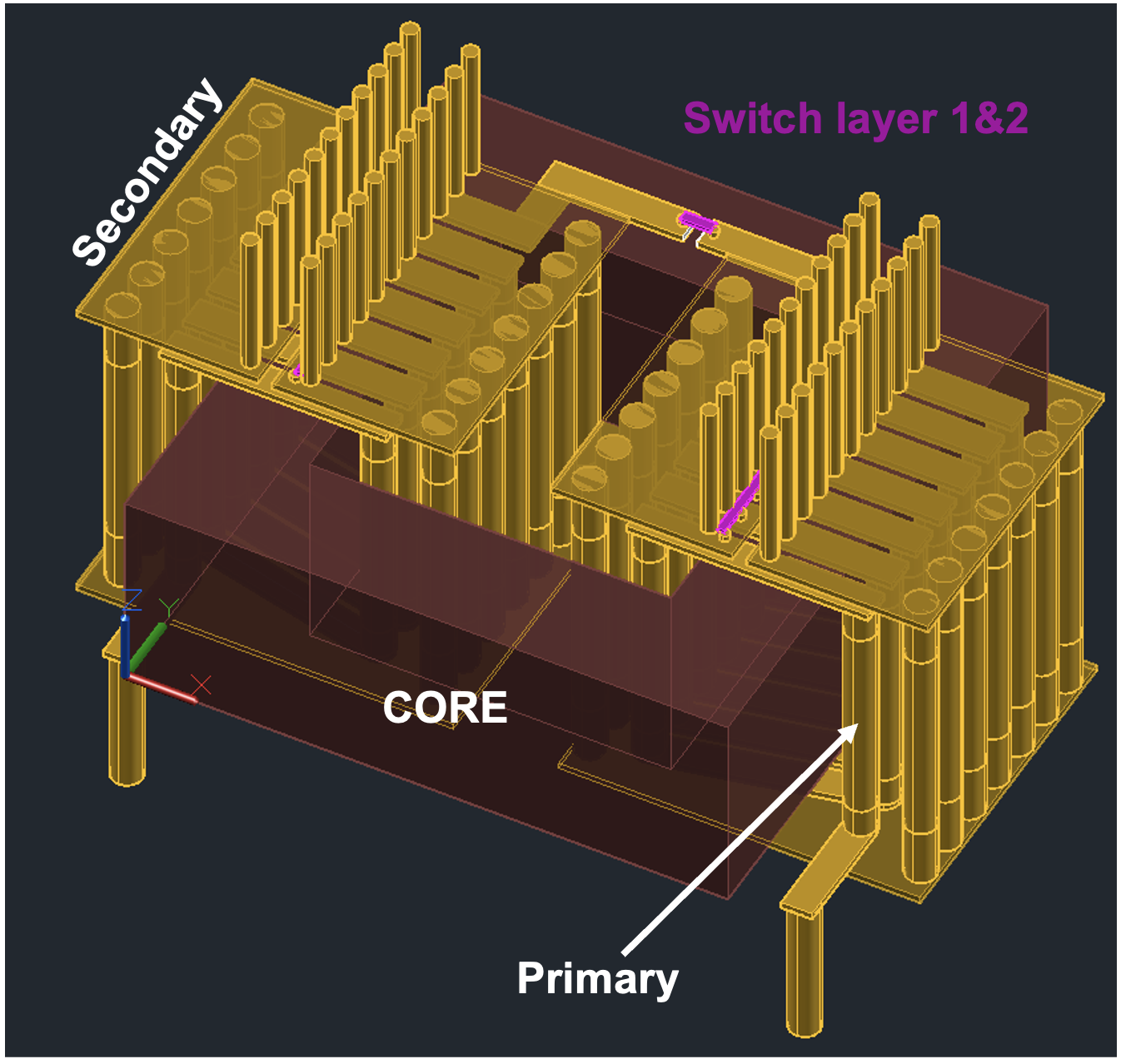
RA2: Integrated micro-transformers for backside power delivery to Wafer Scale Systems (*Ongoing):
Wafer-scale systems for HPC and AI/ML, especially those based on chiplets, are now demanding unprecedented power—up to 50 kW per wafer or substrate—at extreme power densities greater than 1 W/mm². To efficiently deliver such massive power, conventional front-side power delivery methods are not adequate, hence power must be supplied vertically (3D) from the substrate’s backside. Currently, power is delivered to these systems at high voltage (48V) to minimize IR drop and ohmic losses, and then down-converted locally using integrated buck converters or switched capacitors at the point of load; however, this approach is limited to about 80% efficiency (state-of-art) due to conversion losses. In this work, we investigate a fundamentally different approach: distributing high voltage AC, much like conventional power grids, and performing the step-down using integrated micro-transformers within the wafer/substrate. The final regulation and rectification can be managed by integrated power delivery chiplets, enabling both efficient and flexible power delivery across the wafer. We aim to demonstrate that this transformer based power delivery system can achieve significantly better efficiency than current integrated voltage regulator approaches, addressing the extreme power and density demands of next-generation wafer-scale AI/ML and HPC systems.


RA3: Design and Development of custom tool for fiber-array coupling (6-Axis) & attach
Designed a system for attaching optical fiber array modules to photonic chips using multiple coupling schemes. The system comprises an optical table as a base. A sliding mount with an angular orientation mechanism, a laser source to check alignment through an input port, a photodetector to receive the laser beam from the fiber array confirming alignment, a tilt stage, a 3-axis translation stage, a fiber array mounting unit, UV source comprising a UV lamp for attaching a fiber array module to the photonic chip, a first microscope and a second microscope oriented to provide a top and side view of the first vacuum chuck for adjusting position of the chip during attachment. The system is highly cost effective and can hence be easily adopted for prototyping and small-scale product production. The custom tool was used to demonstrate fiber-array coupling and attachment to Si-PICs using Vertical coupling (VGA & QPC) as well as Edge coupling.


Patented system for fiber-array attach

RA4: Design of Photonic System & Package for Quantum Random Number Generator (QRNG) application using Directional Coupler on a Si-PIC:
The focus of this research was on building a True Random Number Generator (TRNG) for quantum cryptographic applications using Silicon Photonics by exploiting the phenomenon of quantum vacuum fluctuations. A simple 3-dB balanced directional coupler with one input arm connected to a highly coherent laser source (1550nm) and other arm kept open will act as a mixer to modulate the input Local Oscillator (LO) signal of the coherent laser with quantum vacuum fluctuations in the open arm, see Figure below for system schematic. The output signals from the two arms of the 3-dB coupler are sent to a balanced photo detector which converts the light to electrical signals followed by differential amplification to remove the LO signal. This differential signal is truly random due to the random nature of vacuum fluctuations and can be digitized using an ADC and sent to an FPGA for post processing (to remove electronically induced signal correlations). The final 8-bit random signal, at a target generation rate of 100 Gbps, can then be used for Quantum Key Distribution (QKD). Some of the key technological aspects of this project are: (i) to design & fabricate a balanced 3dB Si-photonic directional coupler on a 100mm SOI wafer thus making a Photonic Integrated Circuit (PIC), (ii) grating design for coupling light in and out the PIC using optic fibers, (iii) fiber array attachment process for the light coupling, and (iv) full package design including the housing to hold the fiber arrays, TEC, & PIC as well as the DC PCBs for the PIC’s micro-heater control signals and RF PCBs for transmitting the high frequency random signals.


RA5: Thermoelastic modeling of GaN Laser Lift-Off (LLO) Process:
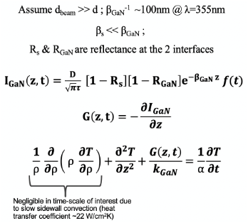
The focus of this research was on trying to model the stresses in GaN thin films grown on c-plane sapphire substrates during the Laser-Liftoff (LLO) process. The LLO process is used to release the thin films of GaN (~5 microns thick) from the sapphire to a target substrate. It is especially used to mass transfer GaN microLEDs to build microLED displays on different substrates & backplanes. During the LLO process, light from a high power, pulsed Excimer or Q-switched solid-state laser (200-350nm wavelength) is passed through the backside of the polished sapphire wafer. Due to the large band gap of sapphire, the light passes through without much absorption. However, when the light hits the GaN/Sapphire interface, the smaller band gap of GaN causes the light pulse to be absorbed. The high power density of the absorbed light causes localized heating and the GaN dissociates into metallic Ga and Nitrogen plasma (ablation). This process happens within a very short timeframe of < 10 nanoseconds and hence there is a thermo-mechanical shockwave created at the GaN/Sapphire interface. The high thermal gradient at the interface as well as the pressure of the expanding nitrogen gas/plasma contribute a dual effect and create a thermo-elastic shockwave that propagates up through the GaN film at the speed of sound. This shockwave can be so intense that it can cause micro-scale cracking of the GaN films especially when the stresses go beyond the yield strength of GaN. Thus, what is experimentally observed is that when the GaN microLEDs undergo LLO process, nearly > 50% of them are cracked thus providing poor process yields. By modeling how this shockwave propagates quantitatively, it is possible to design stress buffer layers on top of the GaN films (Ni layer) to absorb the incoming stress wave so that the peak stresses within the GaN film can be kept below the yield strength at all times. By using this Ni stress buffer layer, the LLO yield was improved to > 99%. This was the main achievement of this research.


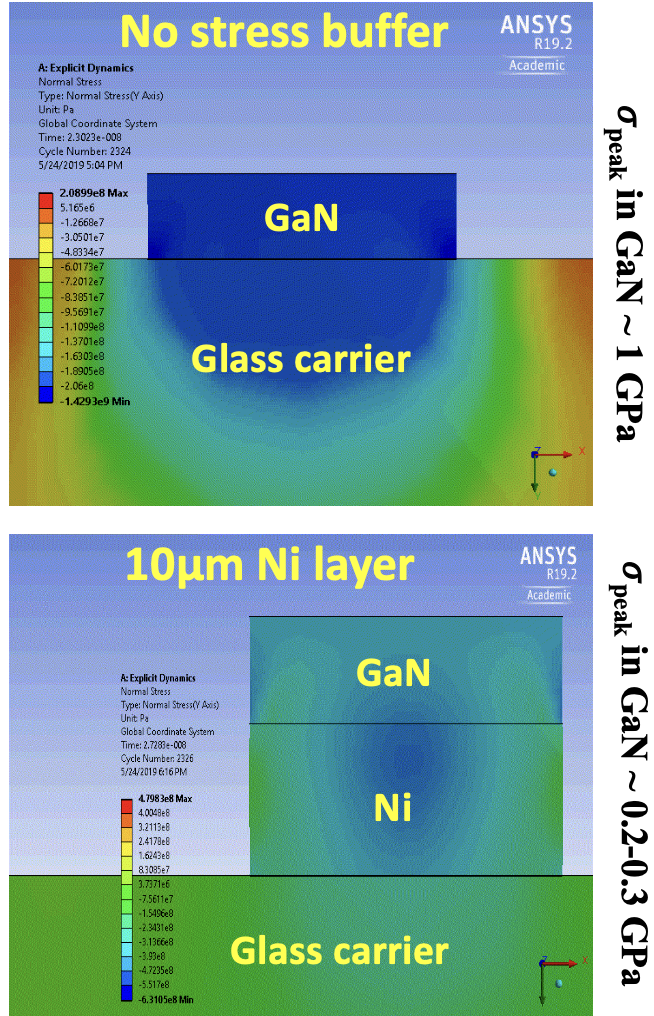


Stress distribution (ANSYS simulation)

RA6: GaN microLED Flexible Display using Fan-Out Wafer-Level Packaging (FOWLP)
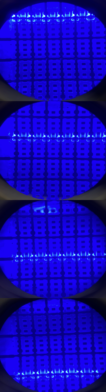
In this work, a die first Fan-Out Wafer-Level Packaging (FOWLP) process called FlexTrate™ is used to heterogeneously integrate GaN blue μLEDs of dimension < 100 μm in a matrix array configuration along with Si-CMOS display driver ICs seamlessly on biocompatible Poly Di-Methyl Siloxane (PDMS) substrates to fabricate a flexible display. The GaN μLEDs, prefabricated on c-plane sapphire substrates, are released using Laser Lift-Off (LLO) with a Diode Pumped Solid State (DPSS) laser source and assembled on the flexible substrate using a novel high yield (> 99%) mass transfer technique based on thermoplastic adhesive bonding. The assembled μLED matrix array on PDMS has a pixel resolution of > 200 PPI. Electrical characterization of the μLEDs at different process stages indicates no significant degradation in operation.


Line-scan operation
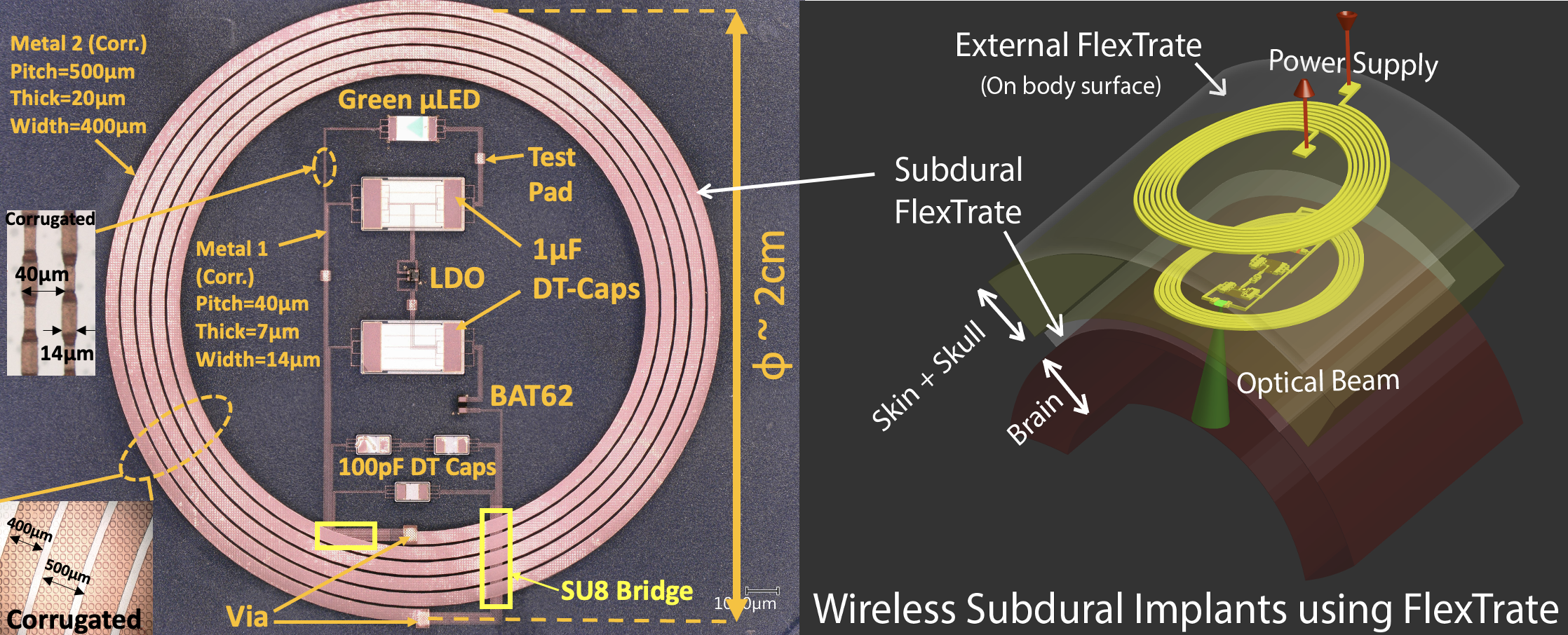
RA7: A Heterogeneously Integrated Wireless Power Transfer (WPT) system using Fan-Out Wafer-Level Packaging (FOWLP)
Fan-Out Wafer-Level Packaging (FOWLP) is used to fabricate a near field, resonantly coupled (13.56 MHz), implantable, wireless power transfer system on an ultra-flexible (~5mm bending radius) & biocompatible elastomeric substrate made of PDMS. A μLED is powered wirelessly with an efficiency > 15% at a 1cm transmit distance to demonstrate device functionality. All components integrated on the flexible package are off the shelf. The heterogeneously-integrated implantable system is only ~ 535μm thick with a diameter < 2cm. Such small form factors are only possible through the use of advanced packaging techniques like FOWLP.


© Goutham Ezhilarasu